
English
English
Tags:
Semiconductor
Nanomaterials
Perovskite
Powder Coating
TEM/FIB sample preparation
Product Description
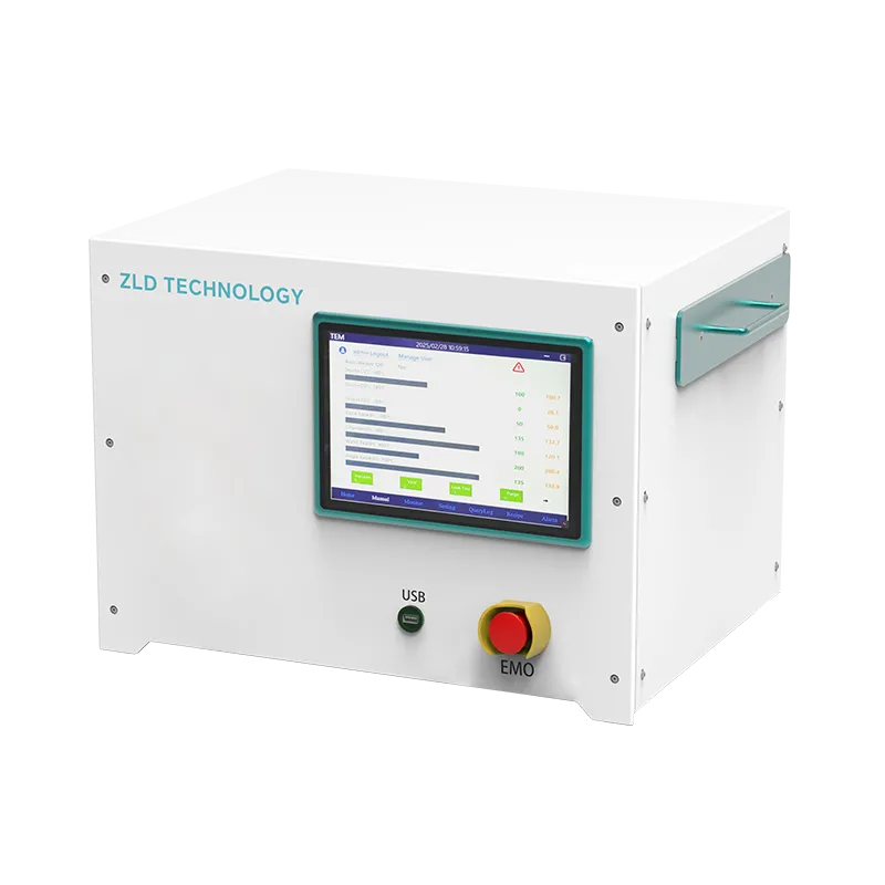
Desktop ALD System by ZLD Technology is a compact, high-precision Atomic Layer Deposition Equipment designed specifically for R&D applications. Engineered with advanced ALD technology, this desktop system offers researchers full control over deposition parameters while maintaining excellent film uniformity and repeatability. Ideal for universities, laboratories, and materials research centers, it enables efficient thin-film coating on wafers and smaller chips — making it an essential tool for innovation in nanotechnology, semiconductors, and energy materials.
1. Compact, quiet, user-friendly
2. Uniform and controllable ALD
3. Sample loading of 4/6 Inch or gram-level powder
4. Full automated human-machine operation interface
5. 4 sets of quick-release precursor modules, wafer drawer loading
6. Optimal R&D solution for advanced energy materials and novel nanomaterials
Oxides: Al₂O₃, SiO₂, TiO₂, ZnO, ZrO₂, HfO₂, Ta₂O₅, MgO, etc.
Nitrides: AlN, TiN, ZrN, HfN, WN
Metals: Ru, Pd, Pt, Ni, Co, W
Sulfides: MoS₂, WS₂, ZnS, TiS₂
TEM Sample Decoration: Desktop ALD can create a clear boundary for TEM imaging via high quality atomically ultra thin coating,develop high Z-contrast coating for TEM imaging, and grow conform 3D authentic decoration coating at low temperature 40-80°C.
Specification
| Dimension(L x W x H) | 590 x 470 x 470 (mm) |
| Weight | 70KG |
| Power Supply | 220VAC 50HZ rating:1.5kW/7A,Peak power 2.2kW/10A |
| Sample Size | Up to 6 inch wafer and smaller chips compatible;Sample height≤3mm |
| Ultimate Vacuum | ≤50 mTorr |
| Process Temperature | RT 360°C |
| Precursor temperature | Maximum 180°C |
| Coating Uniformity | |
| Step Coverage | Deposit on all surfaces with high aspect ratio |
| Sample Handling | Wafers require careful support; powders may require holders or trays to ensure uniform exposure and prevent contamination or aggregation |
Application
1. Energy material
2. Nanomaterials
3. Semiconductors
4. Sensors
Related FAQs

RELATED PRODUCTS

This system includes four process chambers: load-lock (pre-treatment) chamber, ion milling chamber, evaporator, oxidation chamber. Specially designed manipulator allows tilting and rotation of wafer with little friction. Fully automatic operation guarantee reproducible results. QBT-J is the advanced solution to tunneling junction, optical structure, metal-insulator-metal structure, capacitor and so on.
Learn More
It is the world's smallest Atomic Layer Deposition equipment for university, laboratory, which can realize controllable atomic layer deposition on 4/6-inch wafers and micro and nanopowders in high uniformity. It is the the best solution to research and application of advanced energy materials and new nanomaterials.
Learn More
Multi-Chamber UHV Magnetron Sputter
The system can be optionally configured with multiple chambers, including one load-lock chamber and multiple sputtering chambers. It is the cutting edge vacuum system for novel materials. It supports Magnetron Sputtering for ITO Film and Seed Layer Based Process.
Learn More
PEALD realises low temperature, high quality plasma-enhanced ALD processes for high-quality thin film deposition (e.g., SiO₂, Al₂O₃, TiO₂) on various substrates, including lens, glass, organic materials, polymers, metals, and ceramics.
Learn More
ZLD Technology’s Thermal Batch ALD system leverages advanced Thermal Atomic Layer Deposition technology to deliver high-precision thin film deposition for industrial applications.It is a dedicated themal ALD designed for 4/6-inch LED manufacturing lines, comprising process chamber, motion control system and load/unload platform.
Learn More
The upgraded equipment adopts an exclusive design for double‑sided coating, enabling simultaneous and uniform deposition on both sides of the sample without the need for secondary flipping. This greatly improves production efficiency and film uniformity, making it suitable for high‑end applications with strict requirements on double‑sided film performance.It is also equipped with a fully automatic wafer handling system, realizing unmanned sample transfer throughout the process. This not only enhances operational efficiency but also fundamentally eliminates contamination risks caused by manual handling.
Learn More
It enables uniform and precisely controlled ALD or MLD on micro-nano powders, featuring patented powder containers, dynamic powder fluidization mechanisms, fully automated temperature control. The capacity is up to 100 g/1000 g.
Learn More
1. The smallest desktop ALD for R&D, weighing just 50 kg
2. The most widely used applications: Semiconductor, High-K dielectrics, Nanocatalyst, Perovskite, Nanomaterials